Proof, not promises.

Boards our engine designed end to end, the checks every design must pass, and the rules and files you can expect.

Reference boards

Designed automatically. Verified against the rules.

These boards run through the full pipeline on every platform update. Each one has to finish with zero electrical rules errors, zero design rules errors and nothing left unrouted.

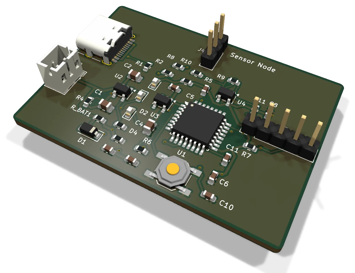
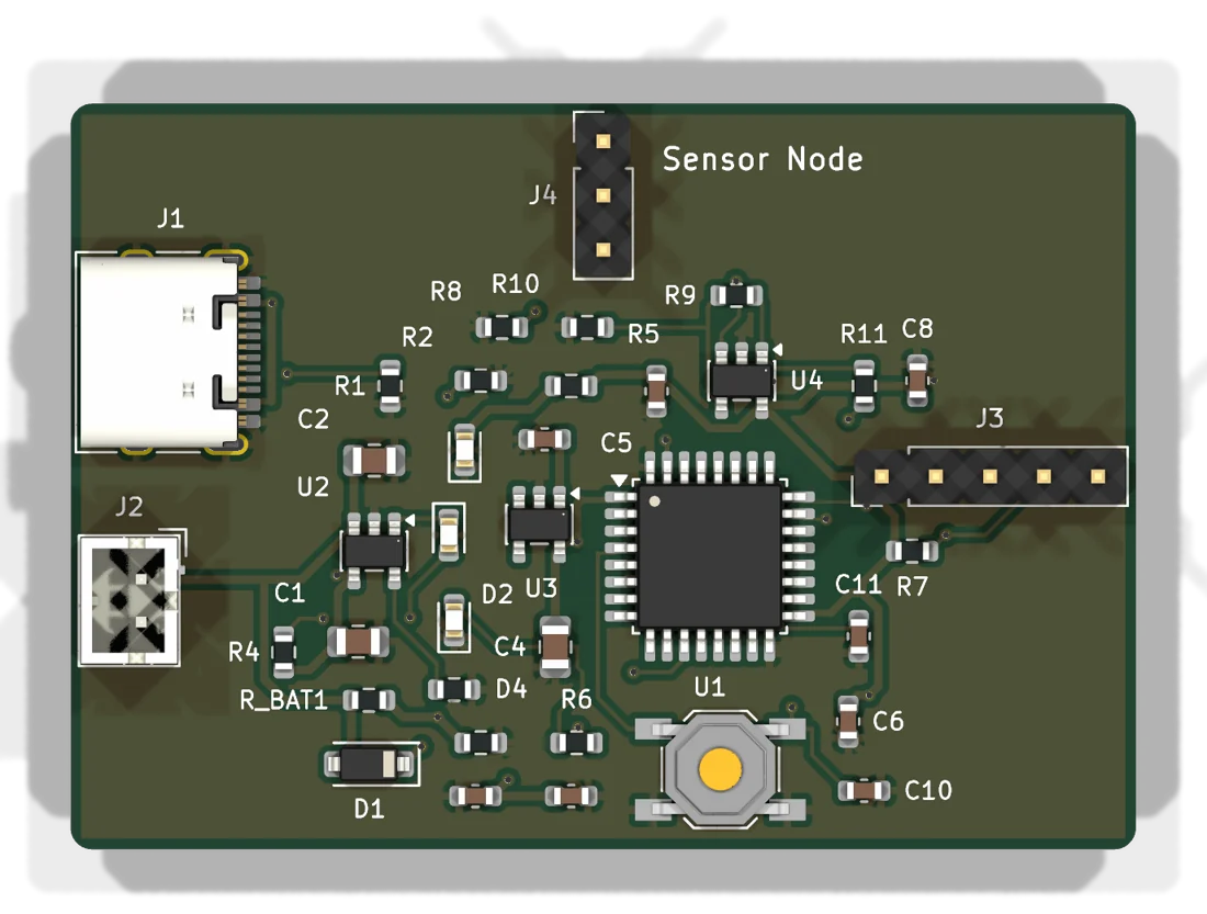
3D render of the sensor node board Top view of the sensor node board
ERC 0 · DRC 0 · 0 unrouted

Battery sensor node

Low-power microcontroller board that charges a LiPo cell from USB-C and reads an analog sensor through an op-amp front end, with status LEDs and an SWD header.

Board
50 × 35 mm
Layers
2
Parts
37
Vias
28
Track segments
309
ERC and DRC
Passed
STM32L031K6T6MCP73831AP2112K-3.3MCP6001USB-CJST PH
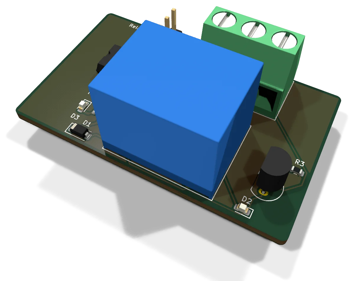
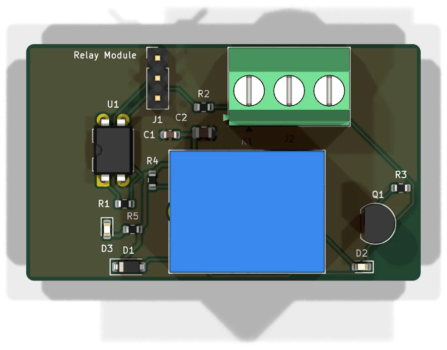
3D render of the relay module board Top view of the relay module board
ERC 0 · DRC 0 · 0 unrouted

Opto-isolated relay module

A 5 V relay driven through an optocoupler and transistor, with a flyback diode, status LEDs and a screw terminal for the switched load.

Board
50 × 30 mm
Layers
2
Parts
15
Vias
0
Track segments
88
ERC and DRC
Passed
SRD-05VDC-SL-CPC817S80501N4148WPhoenix MKDS 5.08
Quality gates

Errors block the next step. Always.

Warnings can be accepted. Errors, missing parts and mismatched parts can never be waived.

1.3 · 2.1

Library match

Every part maps to a verified symbol and an IPC-7351 footprint, and their pins must agree.

2.2

Ratings

Voltage, current, power and thermal margin checked for every part against its role in the circuit.

3.3

ERC + parity

An electrical rules check, plus a check that the drawn schematic matches the intended netlist exactly.

4.1

Placement

The board can grow to fit its parts, never shrink below what they need. Parts may not overlap.

4.3

DRC + unrouted

A design rules check on the routed board against the fabrication rules. A single unrouted connection is an error.

5.2

Safety review

Mains and high-voltage designs need a recorded engineer sign-off before they can be released.

Default design rules

Made for standard fabrication.

RuleValue
Signal track / spacing0.20 / 0.20 mm
Power track0.40 mm
Minimum track / spacing0.10 / 0.127 mm (4+ layers: 0.09 / 0.09 mm)
Via diameter / drill0.60 / 0.30 mm
Copper to board edge0.30 mm
Mains clearance (IPC-2221B)2.5 mm
Layer counts1, 2, 4, 6
Release package

Everything the factory asks for.

FileFormat
Gerbers and drillZIP
Bill of materialsXLSX · JLCPCB CSV
Pick-and-placeXLSX · JLCPCB CSV
SchematicPDF
NetlistNative · XLSX · CSV · JSON
Editable design project with librariesZIP
3D boardGLB
IPC2221 spacing and 7351 land patterns
0Automated checks per design
0Verified schematic symbols
0Verified PCB footprints
Your board next

See your own design pass the same checks.

Start in the studio, or send your files for a review and quote.